| |
|

|
|
|
|
| |
|

|
| |
 |
Introduction
|
|
|
Verilog has built in primitives like gates, transmission gates, and switches. These are rarely used in design (RTL Coding), but are used in post synthesis world for modeling the ASIC/FPGA cells; these cells are then used for gate level simulation, or what is called as SDF simulation. Also the output netlist format from the synthesis tool, which is imported into the place and route tool, is also in Verilog gate level primitives. |
| |
|

|
|
|
Note : RTL engineers still may use gate level primitivies or ASIC library cells in RTL when using IO CELLS, Cross domain synch cells. |
| |
|

|
| |
 |
Gate Primitives
|
| |
|

|
|
|
 |
| |
|

|
|
|
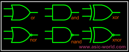
The gates have one scalar output and multiple scalar inputs. The 1st terminal in the list of gate terminals is an output and the other terminals are inputs. |
| |
|

|
|
|
|
Gate
|
Description
|
|
and
|
N-input AND gate
|
|
nand
|
N-input NAND gate
|
|
or
|
N-input OR gate
|
|
nor
|
N-input NOR gate
|
|
xor
|
N-input XOR gate
|
|
xnor
|
N-input XNOR gate
|
|
| |
|

|
| |
 |
Examples
|
| |
|

|
|
|
  1 module gates();
  2
  3 wire out0;
  4 wire out1;
  5 wire out2;
  6 reg  in1,in2,in3,in4;
  7
  8 not U1(out0,in1);
  9 and U2(out1,in1,in2,in3,in4);
 10 xor U3(out2,in1,in2,in3);
 11
 12 initial begin
 13   $monitor(
 14   "in1=%b in2=%b in3=%b in4=%b out0=%b out1=%b out2=%b",
 15    in1,in2,in3,in4,out0,out1,out2);
 16   in1 = 0;
 17   in2 = 0;
 18   in3 = 0;
 19   in4 = 0;
 20    #1  in1 = 1;
 21    #1  in2 = 1;
 22    #1  in3 = 1;
 23    #1  in4 = 1;
 24    #1  $finish;
 25 end
 26
 27 endmodule
You could download file gates.v here
|
| |
|

|
|
|
 in1 = 0 in2 = 0 in3 = 0 in4 = 0 out0 = 1 out1 = 0 out2 = 0
 in1 = 1 in2 = 0 in3 = 0 in4 = 0 out0 = 0 out1 = 0 out2 = 1
 in1 = 1 in2 = 1 in3 = 0 in4 = 0 out0 = 0 out1 = 0 out2 = 0
 in1 = 1 in2 = 1 in3 = 1 in4 = 0 out0 = 0 out1 = 0 out2 = 1
 in1 = 1 in2 = 1 in3 = 1 in4 = 1 out0 = 0 out1 = 1 out2 = 1
|
| |
|

|
| |
 |
Transmission Gate Primitives
|
|
|
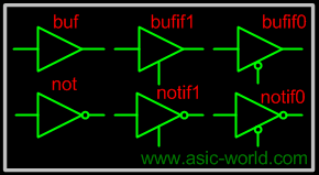
Transmission gates are bi-directional and can be resistive or non-resistive. |
| |
|

|
|
|
Syntax: keyword unique_name (inout1, inout2, control); |
| |
|

|
|
|
 |
| |
|

|
|
|
|
Gate
|
Description
|
|
not
|
N-output inverter
|
|
buf
|
N-output buffer.
|
|
bufif0
|
Tri-state buffer, Active low en.
|
|
bufif1
|
Tri-state buffer, Active high en.
|
|
notif0
|
Tristate inverter, Low en.
|
|
notif1
|
Tristate inverter, High en.
|
|
| |
|

|
|
|
Transmission gates tran and rtran are permanently on and do not have a control line. Tran can be used to interface two wires with seperate drives, and rtran can be used to weaken signals. |
| |
|

|
| |
 |
Examples
|
| |
|

|
|
|
  1 module transmission_gates();
  2
  3 reg data_enable_low, in;
  4 wire data_bus, out1, out2;
  5
  6 bufif0 U1(data_bus,in, data_enable_low);
  7 buf  U2(out1,in);
  8 not U3(out2,in);
  9
 10 initial begin
 11   $monitor(
 12     "@%g in=%b data_enable_low=%b out1=%b out2= b data_bus=%b",
 13     $time, in, data_enable_low, out1, out2, data_bus);
 14   data_enable_low = 0;
 15   in = 0;
 16    #4  data_enable_low = 1;
 17    #8  $finish;
 18 end
 19
 20 always  #2  in = ~in;
 21
 22 endmodule
You could download file transmission_gates.v here
|
| |
|

|
|
|
 @0 in = 0 data_enable_low = 0 out1 = 0 out2 = 1 data_bus = 0
 @2 in = 1 data_enable_low = 0 out1 = 1 out2 = 0 data_bus = 1
 @4 in = 0 data_enable_low = 1 out1 = 0 out2 = 1 data_bus = z
 @6 in = 1 data_enable_low = 1 out1 = 1 out2 = 0 data_bus = z
 @8 in = 0 data_enable_low = 1 out1 = 0 out2 = 1 data_bus = z
 @10 in = 1 data_enable_low = 1 out1 = 1 out2 = 0 data_bus = z
|
| |
|

|
|
|
|
| |
|

|
| |
 |
Switch Primitives
|
|
|
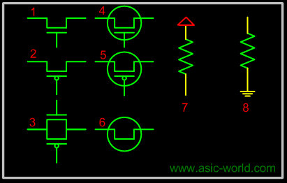
There are six different switch primitives (transistor models) used in Verilog, nmos, pmos and cmos and the corresponding three resistive versions rnmos, rpmos and rcmos. The cmos type of switches have two gates and so have two control signals. |
| |
|

|
|
|
Syntax: keyword unique_name (drain. source, gate) |
| |
|

|
|
|
 |
| |
|

|
|
|
|
Gate
|
Description
|
|
1. pmos
|
Uni-directional PMOS switch
|
|
1. rpmos
|
Resistive PMOS switch
|
|
2. nmos
|
Uni-directional NMOS switch
|
|
2. rnmos
|
Resistive NMOS switch
|
|
3. cmos
|
Uni-directional CMOS switch
|
|
3. rcmos
|
Resistive CMOS switch
|
|
4. tranif1
|
Bi-directional transistor (High)
|
|
4. tranif0
|
Bi-directional transistor (Low)
|
|
5. rtranif1
|
Resistive Transistor (High)
|
|
5. rtranif0
|
Resistive Transistor (Low)
|
|
6. tran
|
Bi-directional pass transistor
|
|
6. rtran
|
Resistive pass transistor
|
|
7. pullup
|
Pull up resistor
|
|
8. pulldown
|
Pull down resistor
|
|
| |
|

|
|
|
Transmission gates are bi-directional and can be resistive or non-resistive. Resistive devices reduce the signal strength which appears on the output by one level. All the switches only pass signals from source to drain, incorrect wiring of the devices will result in high impedance outputs. |
| |
|

|
| |
 |
Examples
|
| |
|

|
|
|
 1 module switch_primitives();
 2
 3 wire  net1, net2, net3;
 4 wire  net4, net5, net6;
 5
 6 tranif0 my_gate1 (net1, net2, net3);
 7 rtranif1 my_gate2 (net4, net5, net6);
 8
 9 endmodule
You could download file switch_primitives.v here
|
| |
|

|
|
|
Transmission gates tran and rtran are permanently on and do not have a control line. Tran can be used to interface two wires with separate drives, and rtran can be used to weaken signals. Resistive devices reduce the signal strength which appears on the output by one level. All the switches only pass signals from source to drain, incorrect wiring of the devices will result in high impedance outputs. |
| |
|

|
| |
 |
Logic Values and signal Strengths
|
|
|
The Verilog HDL has got four logic values |
| |
|

|
|
|
|
Logic Value
|
Description
|
|
0
|
zero, low, false
|
|
1
|
one, high, true
|
|
z or Z
|
high impedance, floating
|
|
x or X
|
unknown, uninitialized, contention
|
|
| |
|

|
| |
 |
Verilog Strength Levels
|
| |
|

|
|
|
|
Strength Level
|
Specification Keyword
|
|
7 Supply Drive
|
supply0 supply1
|
|
6 Strong Pull
|
strong0 strong1
|
|
5 Pull Drive
|
pull0 pull1
|
|
4 Large Capacitance
|
large
|
|
3 Weak Drive
|
weak0 weak1
|
|
2 Medium Capacitance
|
medium
|
|
1 Small Capacitance
|
small
|
|
0 Hi Impedance
|
highz0 highz1
|
|
| |
|

|
| |
 |
Example : Strength Level
|
| |
|

|
|
|
 |
| |
|

|
|
|
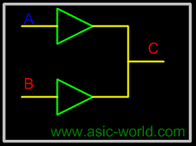
Two buffers that has output |
|
|
A : Pull 1 |
|
|
B : Supply 0 |
|
|
Since supply 0 is stronger then pull 1, Output C takes value of B. |
| |
|

|
| |
 |
Example 2 : Strength Level
|
| |
|

|
|
|
 |
| |
|

|
|
|
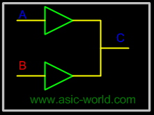
Two buffers that has output |
|
|
A : Supply 1 |
|
|
B : Large 1 |
|
|
Since Supply 1 is stronger then Large 1, Output C takes the value of A |
| |
|

|
| |
|

|
| |
|

|
|
|
|
| |
|

|