| |
|

|
|
|
|
| |
|
|
| |
 |
Introduction
|
|
|
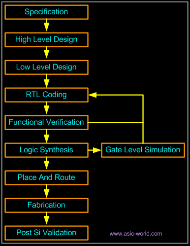
Being new to Verilog you might want to try some examples and try designing something new. I have listed the tool flow that could be used to achieve this. I have personally tried this flow and found this to be working just fine for me. Here I have taken only the front end design part and bits of FPGA design of the tool flow, that can be done without any fat money spent on tools. |
| |
|
|
| |
|
Various stages of ASIC/FPGA
|
|
|
- Specification : Word processor like Word, Kwriter, AbiWord, Open Office.
- High Level Design : Word processor like Word, Kwriter, AbiWord, for drawing waveform use tools like waveformer or testbencher or Word, Open Office.
- Micro Design/Low level design: Word processor like Word, Kwriter, AbiWord, for drawing waveform use tools like waveformer or testbencher or Word.
- RTL Coding : Vim, Emacs, conTEXT, HDL TurboWriter
- Simulation : Modelsim, VCS, Verilog-XL, Veriwell, Finsim, Icarus.
- Synthesis : Design Compiler, FPGA Compiler, Synplify, Leonardo Spectrum. You can download this from FPGA vendors like Altera and Xilinx for free.
- Place & Route : For FPGA use FPGA' vendors P&R tool. ASIC tools require expensive P&R tools like Apollo. Students can use LASI, Magic.
- Post Si Validation : For ASIC and FPGA, the chip needs to be tested in real environment. Board design, device drivers needs to be in place.
|
| |
|
|
| |
 |
Figure : Typical Design flow
|
| |
|
|
|
|
 |
| |
|
|
| |
|
Specification
|
|
|
This is the stage at which we define what are the important parameters of the system/design that you are planning to design. A simple example would be: I want to design a counter; it should be 4 bit wide, should have synchronous reset, with active high enable; when reset is active, counter output should go to "0". |
| |
|
|
| |
|
High Level Design
|
|
|
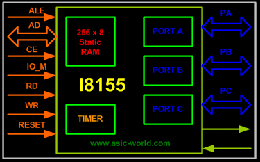
This is the stage at which you define various blocks in the design and how they communicate. Let's assume that we need to design a microprocessor: high level design means splitting the design into blocks based on their function; in our case the blocks are registers, ALU, Instruction Decode, Memory Interface, etc. |
| |
|
|
|
|
 |
|
|
Figure : I8155 High Level Block Diagram |
| |
|
|
|
|
|
| |
|
|
| |
|
Micro Design/Low level design
|
|
|
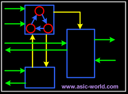
Low level design or Micro design is the phase in which the designer describes how each block is implemented. It contains details of State machines, counters, Mux, decoders, internal registers. It is always a good idea to draw waveforms at various interfaces. This is the phase where one spends lot of time. |
| |
|
|
|
|
 |
|
|
Figure : Sample Low level design |
| |
|
|
| |
|
RTL Coding
|
|
|
In RTL coding, Micro design is converted into Verilog/VHDL code, using synthesizable constructs of the language. Normally we like to lint the code, before starting verification or synthesis. |
| |
|
|
|
|
  1 module addbit (
  2 a      , // first input
  3 b      , // Second input
  4 ci     , // Carry input
  5 sum    , // sum output
  6 co       // carry output
  7 );
  8 //Input declaration
  9 input a;
 10 input b;
 11 input ci;
 12 //Ouput declaration
 13 output sum;
 14 output co;
 15 //Port Data types
 16 wire  a;
 17 wire  b;
 18 wire  ci;
 19 wire  sum;
 20 wire  co;
 21 //Code starts here
 22 assign {co,sum} = a + b + ci;
 23
 24 endmodule // End of Module addbit
You could download file addbit.v here
|
| |
|
|
| |
|
Simulation
|
|
|
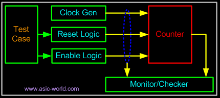
Simulation is the process of verifying the functional characteristics of models at any level of abstraction. We use simulators to simulate the Hardware models. To test if the RTL code meets the functional requirements of the specification, we must see if all the RTL blocks are functionally correct. To achieve this we need to write a testbench, which generates clk, reset and the required test vectors. A sample testbench for a counter is shown below. Normally we spend 60-70% of time in design verification. |
| |
|
|
|
|
 |
|
|
Figure : Sample Testbench Env |
| |
|
|
|
|
We use the waveform output from the simulator to see if the DUT (Device Under Test) is functionally correct. Most of the simulators come with a waveform viewer. As design becomes complex, we write self checking testbench, where testbench applies the test vector, then compares the output of DUT with expected values. |
| |
|
|
|
|
There is another kind of simulation, called timing simulation, which is done after synthesis or after P&R (Place and Route). Here we include the gate delays and wire delays and see if DUT works at rated clock speed. This is also called as SDF simulation or gate level simulation. |
| |
|
|
|
|
 |
|
|
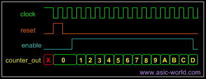
Figure : 4 bit Up Counter Waveform |
| |
|
|
| |
|
Synthesis
|
|
|
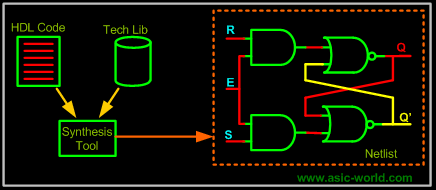
Synthesis is the process in which synthesis tools like design compiler or Synplify take RTL in Verilog or VHDL, target technology, and constrains as input and maps the RTL to target technology primitives. Synthesis tool, after mapping the RTL to gates, also do the minimal amount of timing analysis to see if the mapped design is meeting the timing requirements. (Important thing to note is, synthesis tools are not aware of wire delays, they only know of gate delays). After the synthesis there are a couple of things that are normally done before passing the netlist to backend (Place and Route) |
| |
|
|
|
|
- Formal Verification : Check if the RTL to gate mapping is correct.
- Scan insertion : Insert the scan chain in the case of ASIC.
|
| |
|
|
|
|
 |
|
|
Figure : Synthesis Flow |
| |
|
|
| |
|
Place & Route
|
|
|
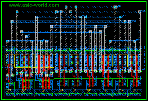
The gatelevel netlist from the synthesis tool is taken and imported into place and route tool in Verilog netlist format. All the gates and flip-flops are placed; clock tree synthesis and reset is routed. After this each block is routed. The P&R tool output is a GDS file, used by foundry for fabricating the ASIC. Backend team normally dumps out SPEF (standard parasitic exchange format) /RSPF (reduced parasitic exchange format)/DSPF (detailed parasitic exchange format) from layout tools like ASTRO to the frontend team, who then use the read_parasitic command in tools like Prime Time to write out SDF (standard delay format) for gate level simulation purposes. |
|
|
 |
|
|
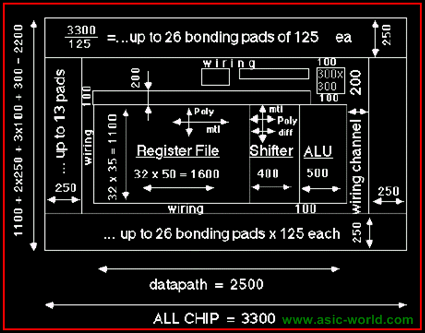
Figure : Sample micro-processor placement |
| |
|
|
|
|
 |
|
|
Figure : J-K Flip-Flop |
| |
|
|
| |
|
Post Silicon Validation
|
|
|
Once the chip (silicon) is back from fab, it needs to be put in a real environment and tested before it can be released into Market. Since the simulation speed (number of clocks per second) with RTL is very slow, there is always the possibility to find a bug in Post silicon validation. |
| |
|
|
| |
|
|
| |
|
|
|
|
|
| |
|
|