|
|
| |
|

|
|
|
|
| |
|

|
| |
 |
Clocking Block
|
|
|
SystemVerilog adds the clocking block that identifies clock signals and captures the timing and synchronization requirements of the blocks being modeled. A clocking block assembles signals that are synchronous to a particular clock and makes their timing explicit. |
| |
|

|
|
|
Clocking block supports following features |
| |
|

|
|
|
- Input sampling
- Synchronous events
- Synchronous drives
|
| |
|

|
|
|
|
| |
|

|
| |
 |
Input and Output Skews
|
|
|
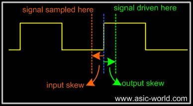
Normally inputs are sampled at clock edge and outputs are driven at clock edge in a cycle based code (Verification and design). If skew is specified, then input is sampled skew time before clock edge and output is driven after the skew time. |
| |
|

|
|
|
This is shown in figure below. A skew must be a constant expression and can be specified as a parameter. If the skew does not specify a time unit, the current time unit is used. If a number is used, the skew is interpreted using the timescale of the current scope. |
| |
|

|
|
|
 |
| |
|

|
| |
|

|
| |
 |
Example : input output skews
|
| |
|

|
|
|
  1 `timescale 1ns/1ns
  2 // program declaration with ports.
  3 program clocking_skew_prg (
  4   input  wire        clk,
  5   output logic [7:0] din,
  6   input  wire  [7:0] dout,
  7   output logic [7:0] addr,
  8   output logic       ce,
  9   output logic       we
 10 );
 11
 12   // Clocking block
 13   clocking ram @(posedge clk);
 14      input   #1  dout;
 15      output  #1  din,addr,ce,we;
 16   endclocking
 17
 18   initial begin
 19     // Init the outputs
 20     ram.addr <= 0;
 21     ram.din <= 0;
 22     ram.ce <= 0;
 23     ram.we <= 0;
 24     // Write Operation to Ram
 25     for (int i = 0; i < 2; i++) begin
 26       @ (posedge clk);
 27       ram.addr <= i;
 28       ram.din <= $random;
 29       ram.ce <= 1;
 30       ram.we <= 1;
 31       @ (posedge clk);
 32       ram.ce <= 0;
 33     end
 34     // Read Operation to Ram
 35     for (int i = 0; i < 2; i++) begin
 36       @ (posedge clk);
 37       ram.addr <= i;
 38       ram.ce <= 1;
 39       ram.we <= 0;
 40       // Below line is same as  @ (posedge clk);
 41       @ (ram);
 42       ram.ce <= 0;
 43     end
 44      #40  $finish;
 45   end
 46
 47 endprogram
 48
 49 // Simple top level file
 50 module clocking_skew();
 51
 52 logic        clk = 0;
 53 wire   [7:0] din;
 54 logic  [7:0] dout;
 55 wire   [7:0] addr;
 56 wire         ce;
 57 wire         we;
 58 reg    [7:0] memory [0:255];
 59
 60 // Clock generator
 61 always  #10  clk++;
 62
 63 // Simple ram model
 64 always @ (posedge clk)
 65  if (ce)
 66    if (we)
 67      memory[addr] <= din;
 68    else
 69      dout <= memory[addr];
 70
 71 // Monitor all the signals
 72 initial begin
 73  $monitor("@%0dns addr :%0x din %0x dout %0x we %0x ce %0x",
 74            $time, addr, din,dout,we,ce);
 75 end
 76 // Connect the program
 77 clocking_skew_prg U_program(
 78  .clk   (clk),
 79  .din   (din),
 80  .dout  (dout),
 81  .addr  (addr),
 82  .ce    (ce),
 83  .we    (we)
 84 );
 85
 86 endmodule
You could download file clocking_skew.sv here
|
| |
|

|
| |
 |
Simulation : input output skews
|
| |
|

|
|
|
 @0ns addr :xx din xx dout xx we x ce x
 @11ns addr :0 din 24 dout xx we 1 ce 1
 @31ns addr :0 din 24 dout xx we 1 ce 0
 @51ns addr :1 din 81 dout xx we 1 ce 1
 @71ns addr :1 din 81 dout xx we 1 ce 0
 @91ns addr :0 din 81 dout xx we 0 ce 1
 @110ns addr :0 din 81 dout 24 we 0 ce 1
 @111ns addr :0 din 81 dout 24 we 0 ce 0
 @131ns addr :1 din 81 dout 24 we 0 ce 1
 @150ns addr :1 din 81 dout 81 we 0 ce 1
 @151ns addr :1 din 81 dout 81 we 0 ce 0
|
| |
|

|
| |
|

|
| |
|

|
|
|
|
| |
|

|
|
|
|

|

|

|
|

|
|
Copyright © 1998-2025 |
Deepak Kumar Tala - All rights reserved |
|
Do you have any Comment? mail me at:deepak@asic-world.com
|
|